- How Does Heterojunction Solar Work?
- Is Heterojunction Solar 26.8% Efficient?
- How Does Heat Affect Heterojunction Solar?
- What Should You Check on a Heterojunction Solar Module?
- Frequently asked questions
- Is HIT the same thing as a heterojunction cell?
- Will a heterojunction module be 26.8% efficient?
- Does a better temperature coefficient always mean more energy?
- Sources and references
Heterojunction solar uses a crystalline silicon wafer with very thin amorphous silicon layers on it. The wafer absorbs the light. The amorphous layers passivate the wafer surface and sort the electrical charges, so the metal contacts are not sitting directly on the absorber. That is the whole idea. The 26.8% figure that appears in efficiency tables is a certified cell result, not the nameplate of a module on a roof.
Updated October 2026. HIT, HJT and SHJ refer to this family. HIT is the older trade name associated with Sanyo, later Panasonic. HJT and silicon heterojunction (SHJ) are the generic names.
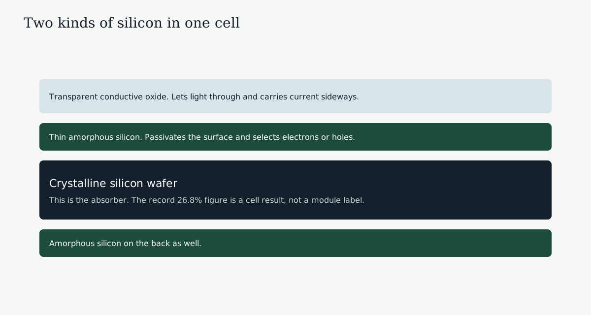
How Does Heterojunction Solar Work?
A conventional crystalline cell forms its junction by diffusing dopant into the wafer itself. A heterojunction cell leaves that wafer as the absorber and puts a different silicon — hydrogenated amorphous silicon — on the surface. An intrinsic amorphous layer passivates the surface. Doped amorphous layers then form the electron-selective and hole-selective contacts. A transparent conductive oxide carries the current sideways to the metal grid, because the amorphous films are too thin and too resistive to do that job alone.
A review of the amorphous-on-crystalline interface, hosted by the US Office of Scientific and Technical Information, ties the high open-circuit voltage of these cells to that passivation. The same paper notes that the metal-to-wafer contact is a serious recombination path in a standard homojunction, and that the amorphous stack is what keeps the metal off the absorber. The wafer process that comes before any of this — ingot, slice, texture — is the subject of how a silicon panel is manufactured. Heterojunction production departs from that story at the junction, not at the melt.
Is Heterojunction Solar 26.8% Efficient?
Version 62 of the solar cell efficiency tables lists a crystalline silicon cell at 26.8% ± 0.4. The area is 274.4 cm², marked as total area. Open-circuit voltage is 0.7514 V, short-circuit current density is 41.45 mA/cm², and fill factor is 86.1%. The table credits an n-type heterojunction cell from LONGi, measured by ISFH in October 2022.
Read the row as a laboratory designation, not as a product. A module adds glass, encapsulant, gaps between cells, and a junction box. Its nameplate efficiency is lower than the best cell inside it, and a datasheet efficiency is measured at standard test conditions, not at the temperature of a roof in July. If a brochure puts 26.8% next to a module wattage, ask which row of which efficiency table they mean.
How Does Heat Affect Heterojunction Solar?
The same interface paper cites published temperature coefficients of about −0.23%/°C to −0.1%/°C for silicon heterojunction cells, against about −0.45%/°C for a standard homojunction and about −0.35%/°C for homojunctions with passivating contacts. Those are cited values, not a rating stamped on every module. The paper then shows why the gap is worth checking: starting from a 20% cell at 25°C, a coefficient difference of 0.12 or 0.35 percentage points per degree produces about a 5.4% or 15.8% relative efficiency difference at 70°C. That arithmetic is their illustration. It is not a yield forecast for a plant.
The practical reading is narrower. Ask the module datasheet for its own temperature coefficient of maximum power, and for the conditions under which it was measured. A hot roof with poor rear ventilation is where a lower coefficient earns its keep. A cool, well-ventilated array will not show the same gap. Do not transfer a cell-paper range onto a module that has not published the number.
What Should You Check on a Heterojunction Solar Module?
The cell architecture does not tell you the module’s fire rating, the mechanical load, the warranty, or whether the bill of materials in the box matches the bill of materials that was certified. Those sit on the module datasheet and the certificate for that model. Low-temperature deposition of the amorphous layers is a manufacturing distinction from a high-temperature diffused junction. A 2019 review describes that deposition as usually below 200°C. Treat that as the review’s process description, and confirm the factory route with the maker if the process temperature is part of a procurement argument.
Bifacial construction is common in this family because the wafer is contacted through thin films on both sides, but a bifacial gain is a site number — albedo, height, row spacing — not a property you can copy from the cell record.
Frequently asked questions
Is HIT the same thing as a heterojunction cell?
HIT is the trade name Sanyo, later Panasonic, used for this architecture. Heterojunction, HJT and SHJ are the generic names for a crystalline wafer with thin amorphous silicon contacts. A module labelled HJT is in that family. It is not automatically a Panasonic product.
Will a heterojunction module be 26.8% efficient?
No. That figure is one certified cell in the version 62 efficiency tables, on 274.4 cm², measured in 2022. A module nameplate is a different measurement, on a full laminate, and it belongs on the datasheet of the model you are buying.
Does a better temperature coefficient always mean more energy?
It means less loss as the cell gets hotter, relative to a cell with a steeper coefficient. The size of the gain depends on how hot the module actually runs. A datasheet coefficient and a site temperature are both required before anyone turns it into kilowatt-hours.
Sources and references
Solar cell efficiency tables, version 62, including the 26.8% n-type heterojunction cell measured by ISFH in October 2022: NLR docs, PDF. Temperature coefficients and the 70°C illustration, in a paper on the amorphous/crystalline interface: OSTI 1229738. Sanyo’s patents and the heterojunction device family: Haschke and colleagues, Materials Science and Engineering R, 2020. Low-temperature deposition as described in a 2019 review: current status of a-Si/c-Si heterojunction cells.
