- The six stages at a glance
- The manufacturing process, step by step
- 1. Purifying silicon into polysilicon
- 2. Growing a single-crystal ingot
- 3. Slicing ingots into wafers
- 4. Turning wafers into solar cells
- 5. Assembling the module
- 6. Testing, grading and certification
- Where solar panels are made
- How much energy does it take to make a solar panel?
- What this means when you buy panels
- Frequently asked questions
- What raw materials are solar panels made from?
- How long does it take to manufacture a solar panel?
- What is the difference between monocrystalline and polycrystalline panels?
- Why are solar cells blue or black?
- Are solar panels recyclable?
- Sources
A solar panel starts as quartz sand and ends as a laminated glass sandwich that is expected to work outdoors for 30 years. In between, the silicon is purified to better than 99.9999%, grown into a single crystal, sliced thinner than a sheet of card, turned into a solar cell in about a dozen chemical and thermal steps, then wired, laminated, framed and tested. Knowing those steps helps buyers understand why two panels with the same wattage can perform very differently.
Short answer: solar panels are manufactured in six stages: (1) quartz is refined into high-purity polysilicon; (2) the polysilicon is melted and grown into a single-crystal ingot; (3) the ingot is sliced into wafers about 130 to 150 µm thick with diamond wire; (4) each wafer is processed into a solar cell by texturing, doping, passivation, coating and printing metal contacts; (5) cells are soldered into strings and laminated between glass and encapsulant, then framed and fitted with a junction box; (6) every panel is flash-tested and electroluminescence-imaged before shipping.
Last updated: October 2026. This guide describes mainstream crystalline silicon panels, which make up the vast majority of the market. Process details follow Fraunhofer ISE, the International Technology Roadmap for Photovoltaics (ITRPV) and the IEA; links are under Sources.
The six stages at a glance
| Stage | Input | What happens | Output |
|---|---|---|---|
| 1. Polysilicon | Quartz, metallurgical silicon | Chemical purification and deposition | Solar-grade polysilicon chunks or granules |
| 2. Ingot | Polysilicon, dopant | Melting and single-crystal pulling (Czochralski) | Cylindrical mono-crystalline ingot |
| 3. Wafer | Ingot | Squaring and diamond-wire slicing | Wafers of roughly 130–150 µm |
| 4. Cell | Wafer | Texturing, doping, passivation, anti-reflection coating, metallization | Solar cell, about 25–27% efficient |
| 5. Module | Cells, glass, encapsulant, frame | Stringing, layup, lamination, framing, junction box | Finished solar panel |
| 6. Testing | Finished panel | Flash test, EL imaging, insulation test, grading | Labelled, certified panel ready to ship |
The manufacturing process, step by step
1. Purifying silicon into polysilicon
Quartz is first reduced with carbon in an arc furnace to make metallurgical-grade silicon, about 98 to 99% pure. That is far too impure for solar cells. Most producers then use the Siemens process: the silicon is converted into a gas, trichlorosilane, which is distilled and then decomposed onto heated silicon rods at around 1,100 °C, building up thick rods of polysilicon. Some producers, notably GCL, also use a fluidized bed reactor that makes small granules instead of rods. The result is solar-grade polysilicon, typically 99.9999% pure or better. This is the most energy-intensive step in the chain.
2. Growing a single-crystal ingot
Polysilicon chunks are melted in a quartz crucible at just above silicon’s melting point of 1,414 °C, with a small amount of dopant added. Today that is usually phosphorus, making n-type silicon for TOPCon, heterojunction and back-contact cells. In the Czochralski method, a seed crystal is dipped into the melt and slowly pulled upward while rotating, so the silicon freezes onto it as one continuous crystal. The result is a cylindrical ingot that can be several metres long. Ingot diameter sets the wafer size: the industry has moved to large formats such as 182 mm (M10) and 210 mm (G12), including rectangular versions.
3. Slicing ingots into wafers
The round ingot is cut into square-sided blocks and then sliced into thousands of wafers at once on a diamond-wire saw, a web of very thin steel wire coated with diamond particles. Wafers are now about 130 to 150 µm thick; Fraunhofer ISE cites 140 µm. Each cut loses about 55 µm of silicon as sawdust (kerf), according to the ITRPV. Thinner wafers and smaller kerf are the main reason silicon use has fallen from about 16 g per watt in 2004 to about 2 g per watt today.
4. Turning wafers into solar cells
Cell making is where most of the efficiency is won or lost. For an n-type TOPCon cell, the most common type in 2026, a typical production flow is:
- Texturing: an alkaline etch removes saw damage and forms microscopic pyramids that trap light.
- Boron diffusion: boron is diffused into the front surface in a furnace to create the p-n junction.
- Rear cleaning and edge isolation: unwanted boron is etched off the rear and edges.
- Tunnel oxide and polysilicon: an oxide layer only 1 to 2 nm thick is grown on the rear, followed by a phosphorus-doped silicon layer, usually by LPCVD or PECVD. This “passivated contact” is what gives TOPCon its name and much of its efficiency.
- Annealing: a high-temperature step (roughly 800 to 1,050 °C) crystallizes the layer and activates the dopants.
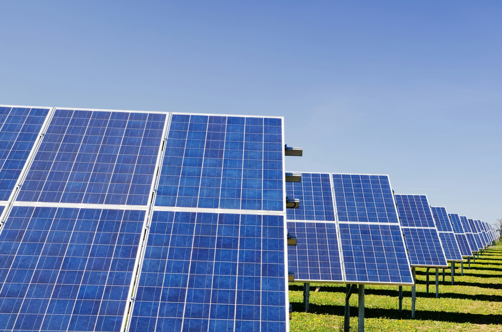
- Passivation and anti-reflection coating: aluminium oxide and silicon nitride layers reduce surface losses and give the cell its dark blue or black colour.
- Metallization: silver-based paste is screen-printed in fine fingers on both sides and fired in a belt furnace.
- Laser contact treatment: many lines add a laser step (LECO) after firing to lower contact resistance.
- Cell testing and sorting: every cell is measured under a flash lamp and sorted into efficiency and colour bins.
Other cell types use different flows. PERC cells, now largely replaced, used aluminium on the rear. Heterojunction (HJT) cells deposit thin amorphous silicon layers at low temperature. Back-contact cells, such as LONGi’s HPBC, move all the metal contacts to the rear so the front has no grid lines. Commercial cells now reach around 25 to 27% efficiency.
5. Assembling the module
Cells are usually laser-cut in half first, which reduces resistive losses and the impact of shading. Then:
- Stringing: automatic stringers solder or bond thin copper ribbons or wires across the cells, linking them into strings.
- Layup: strings are laid on the front glass on top of an encapsulant sheet (EVA, POE or a combination), connected with busbars, and covered with a second encapsulant sheet and either a rear glass or a polymer backsheet.
- Lamination: the stack is heated under vacuum, typically around 145 to 160 °C, so the encapsulant melts and cross-links, sealing the cells and bonding the layers into one unit.
- Framing and junction box: an anodized aluminium frame is fitted with sealant, and the junction box with bypass diodes and output cables with connectors is attached to the rear.
Most utility panels are now dual-glass (2.0 mm glass on each side) and bifacial, collecting light reflected onto the rear. Many residential panels use 3.2 mm front glass with a backsheet. These choices affect weight, durability and how the panel must be mounted.
6. Testing, grading and certification
Every finished panel goes through end-of-line testing:
- Flash (I-V) test: a simulated light pulse at standard test conditions (1,000 W/m², 25 °C) measures power, voltage and current, which sets the panel’s power class on the label.
- Electroluminescence (EL) imaging: current is passed through the panel so the cells glow in infrared; cracks, broken fingers and bad solder joints show up as dark areas.
- Insulation and ground-continuity tests: confirm the panel is electrically safe.
- Visual inspection and grading: panels with defects are downgraded or rejected.
Separately, each panel design must be certified by a test lab, usually to IEC 61215 (performance and durability) and IEC 61730 (safety), or UL 61730 for North America. Independent programmes such as Kiwa PVEL go further: their thermal cycling runs 600 cycles instead of the 200 required for certification, and damp heat 2,000 hours instead of 1,000.
Where solar panels are made
China dominates every stage. The IEA found that China’s share of all the main manufacturing stages exceeded 80%, with 97% of global wafer capacity in 2021, and expected its share of polysilicon, ingots and wafers to approach 95%. The leading manufacturers are profiled in our guide to the top 10 solar panel manufacturers in China. The United States, India, Southeast Asia and Europe have module assembly capacity, but most still rely on imported wafers or cells.
How much energy does it take to make a solar panel?
Making polysilicon and ingots uses the most energy, but a panel repays it quickly. Fraunhofer ISE estimates an energy payback time of about 1.1 years for European-made systems in Northern Europe and about 0.9 years in Southern Europe. Over a 20 to 30-year life, a panel generates many times the energy used to make it.
What this means when you buy panels
Most of what decides a panel’s long-term reliability happens in the factory and is invisible on a datasheet: wafer quality, the encapsulant and glass chosen, lamination control, soldering, and how strictly EL images are checked. Two practical steps help:
- Ask for the exact bill of materials (cell type, glass, encapsulant, backsheet) and the certificate for that configuration and factory.
- Arrange pre-shipment inspection with EL imaging and power sampling, especially on first orders.
Panels also need the right balance-of-system parts. The junction box connector must mate with your field connectors (see solar connector manufacturers and what an MC4 connector is), and string voltage and current must match your DC breakers, isolators and combiner boxes.
Buying solar panels from China?
ShineTong’s sourcing service matches you with established manufacturers, arranges pre-shipment inspection on request, and ships panels together with connectors, cables and DC protection.
Frequently asked questions
What raw materials are solar panels made from?
Mainly silicon (from quartz) for the cells, glass, aluminium for the frame, polymer encapsulant and backsheet, copper ribbons, silver paste for the cell contacts, and a plastic junction box with diodes and cables.
How long does it take to manufacture a solar panel?
Module assembly on an automated line takes well under an hour per panel, with lamination the longest single step. The whole chain from polysilicon to finished panel, including ingot growth, typically takes several days to a few weeks.
What is the difference between monocrystalline and polycrystalline panels?
Monocrystalline panels use wafers cut from a single crystal, giving higher efficiency. Polycrystalline wafers were cast from many crystals and are cheaper but less efficient. Almost all panels made today are monocrystalline.
Why are solar cells blue or black?
The colour comes from the silicon nitride anti-reflection coating and the textured surface. Its thickness is tuned to reflect as little light as possible, which makes cells look dark blue or black.
Are solar panels recyclable?
Yes. Glass, aluminium and copper are readily recovered, and processes exist to recover silicon and silver. Fraunhofer ISE notes that more research is needed to make deeper recycling cost-effective.
Sources
- Fraunhofer ISE, Photovoltaics Report (silicon use, wafer thickness, energy payback time): ise.fraunhofer.de
- ITRPV 15th edition (kerf loss, wafer thickness trends): ITRPV PDF
- Fraunhofer ISE, industrial TOPCon cell process: ise.fraunhofer.de
- PV Tech, towards industrial manufacturing of TOPCon (tunnel oxide, annealing temperatures): pv-tech.org
- PV-Manufacturing.org, TOPCon solar cells: pv-manufacturing.org
- IEA, Solar PV Global Supply Chains: iea.org
- Kiwa PVEL 2026 Scorecard findings: kiwa.com; summary of test durations: parcelandgrid.com